WS2812 Headlight
Last updated: Jan. 31, 2026, 9:29 p.m.
The PCB for this project was sponsored by PCBWay. While I was planning the project anyway, the choice to use their service was based primarily on the offer of a free board.
I'm working on a Hacky Racer, that is an electric go-kart type vehicle for a UK based racing competition. The budget is strictly limited to keep the competition field level, but one of the permitted extras is lights (they come under the safety category). For our racer we decided it would be fun to have some headlights that looked like eyes and could be animated. So while we wait for batteries to arrive for the project, I started a design.
The brief was to have something about 100mm diameter and that could display a range of patterns and animations. I had a reel of standard WS2812B LEDs (like Neopixels) so they seemed like an obvious choice. We want to be able to connect the lights into whatever battery we use so we wanted a wide range of input voltages (at least 12 to 48V), and we want the animation of the lights to be related to the vehicle, maybe they look left and right as we steer, so we needed some sort of comms.
Design
I found the power supply chip first and used TI Webbench to make a design for it. The regulator has a wide input of 7-60V and produces 5V to drive the WS2812 LEDs at up to 5Amp. I think this is over rated on current, but I'm interested in the design for potential battery powered Raspberry Pi 5 projects. From the 5V supply the LEDs are driven directly and the MCU has a follow on 3.3V regulator.
Next I looked at the control, I considered a selection of the cheapest and smallest STM32s but driving animations on arrays of WS2812s is easier with more memory. I thought about using an RP2040 (or RP2350) but the extra layout for the external memory put me off. In the end I settled on the new STM32H523CET6 which is small (only 48 pin), it has loads of memory and a very flexible PLL architecture which makes getting the right clock speed for driving the pixel one wire signal easier. It also gives options for comms, the H5 has a CANFD interface, as well as lots of UARTs.
Next I fleshed out those comms interfaces. I'm not sure what we're going to use on the racer yet but it'll have to be pretty robust. First I added an RS485 transciever attached to a UART peripheral. That's pretty straight forward and something I've used lots before in PiWars motor drivers for example. I also added a CANFD transciever attahced to the CANFD peripheral in the STM32. I've not used CAN in my projects before but it might be something we use on the car because it's popular in automotive stuff. I thought if they were all included on the PCB I could populate as necessary. Both of these interfaces use 120 Ohm twisted pair with shield. I've added the same connector (a pluggable terminal block, I used these on PiWars) and a jumper to optionally include the 120 Ohm termination for each bus. I also added a third pin which is for the shield. Generally the shield is only connected at the bus controller, but having a terminal to join shield on daisy-chained connectors is really useful. From experience with EMC testing and specifically the ESD discharges (static discharges, usually from people with woolly jumpers!) if you have no connection between shield and board ground you can get spikes that upset comms or damage things so as well as a jumper to connect the shield to ground if you want to do that, I added a capacitor and resistor to allow a path for sudden discharges to ground. Typically static discharges are very high voltage, testing is often carried out at 8kV or 15kV. There's very little current so you don't need components rated at this voltage continuously but I did spec these parts at 1kV to keep them robust.
Finally I added the chain of LEDs. WS2812s need a 5V data signal, to make sure the signal was valid for them I added a buffer, it's an LVCT type, the final "T" means it's a TTL-compatible input level, so anything above 2V is a logical 1. That means even when running on 5V it will reliably switch on a 3.3V logic signal. There's a 470 Ohm resistor as recommended for the data line to avoid too much noise from the 5V clock signal. I also added a decoupling cap next to each LED. I didn't bother with a bulk capacitor as you see in some designs because I had such a big regulated power supply right on the board.
Layout
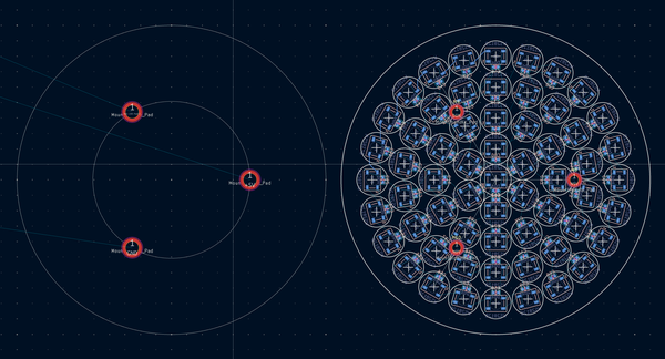
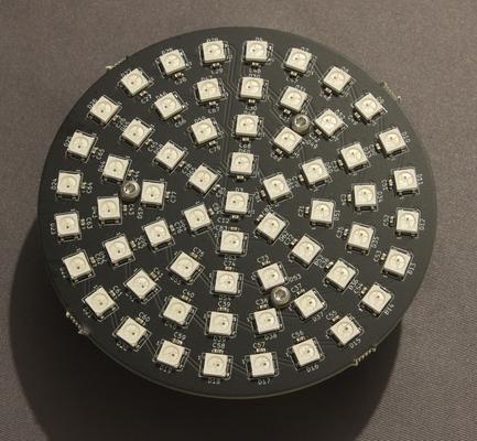
With all the design in place I pushed it over to the PCB and started to think about layout. Initially I had some LEDs but I hadn't figured out how many I'd use yet. The first thing I tackled was the LED array. I wanted to fill a 100mm disk as neatly as possible. First I tried a rectangular array but with decoupling caps the LED block was about 10mm across, this left a lot of empty spaces in the curves of the circle, it was more of a cross than a circle. A circular layout would have been difficult in just KiCAD but it has excellent import tools for DXF. I used LibreCAD which is a 2D design tool I've used a lot. I drew a sequence of circles and radial spokes which is easy with the tools it provides. At the intersection of each I left a little cross (again easy with the layoout and snap tools in LibreCAD). I exported this little constellation of crosses as a DXF and then imported them into KiCAD. In KiCAD with the layer I imported to them active when I move an LED its centre point snaps to the little cross I made. I rotated the LEDs to match their location to make a clean circular pattern then I finally rotated all the capacitors to match and placed one next to each LED. As I progressed through this process I figured out how many LEDs I actually needed and extended the array in the schematic to match.
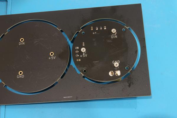
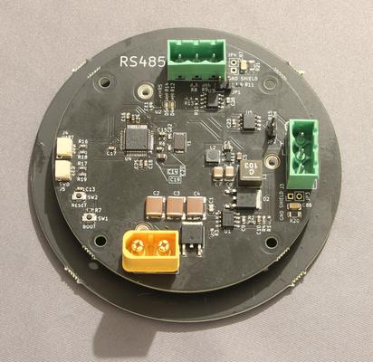
I wanted to use the bulky plug in terminals for comms because they're easy to wire up, and a standard XT60 connector for the battery bus voltage. All these parts were through hole and I couldn't fit them inbetween the LEDs without upsetting my neat pattern. I decided to make it a 2 board design. That means I've got a whole board just for the power and logic and a whole board to get my LEDs exactly where I want them. This makes it a bit bigger and to get 2 boards made at a time I'll have to do a panel design which needs some extra work on the board edge design. I need to get 3 signals from the bottom (control) to the top (LED) board, +5V, GND and the data signal. I also need to support the two boards mechanically. I decided to put 4 mounting holes on the bottom board for mounting it to whatever support structure I design later. Between the boards I've used a trio of solder down standoff pillars. These solder into one side and have a thread down the middle to take a bolt. It makes it easier than having to use a nut and bolt or short bolts that don't meet in the middle of a through threaded pillar. These three pillars can also be the electrical connectors, one for each signal. I picked M2.5 pillars and bolts which seemed to fit between the pixels okay. You can go down to M2 with these parts but I didn't want it too fragile given the harsh environment it was likely to experience.
I laid out the board with the LEDs on the bottom the controls on the top. That way the layout was like it will all be in real life, I didn't have to get confused about mirroring the pillar locations on the two boards, they matched because the boards were designed to stack. I laid out the power supply for the bottom board first based on the datasheet for the chip which had detailed layout notes. I squeezed this design into the board between all the holes and found a good place to put the big XT60 connector and assigned the pillars based on where the power supply was. With that critical section done I spread the MCU and comms interfaces around making sure to leave good clearance around the mounting holes.
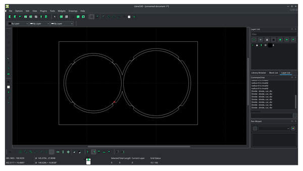
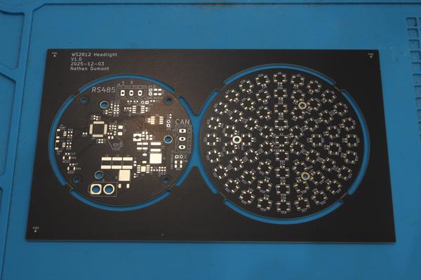
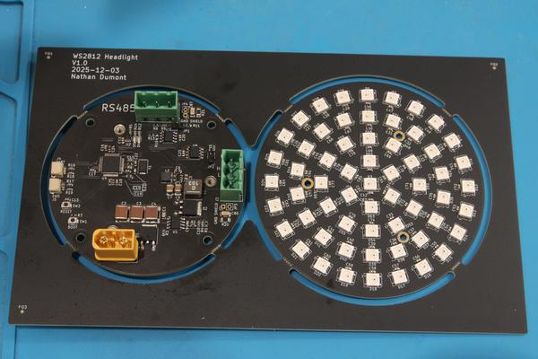
The last part of the puzzle was to make the two separate circles into a panel I could order as a single item. You can order it as separates but as I always want to use these two boards together making a panel makes sense. When I panelised the design I flipped the whole top board so the LEDs were on the top layer. That means I've only got the three solder in pillars on the back which I can easily solder by hand so now I only need 1 paste stencil for the top side which saves me money and time. I used LibreCAD again to do the board outlines. I included the two circles inside a rectangular frame and added mousebites across a 3mm routing gap with rounded ends. I added the drill holes for the mousebites as tiny circles (0.5mm, well within PCBWay's capabilities for unplated holes). You could use a footprint to make the holes but you generally want the mousebite holes unplated so a via wouldn't do.
I added some fiducials to the frame, if I had a pick and place machine these would help get the board lined up with the machine, the frame is a good place to put these kind of manufacturing related things because they are well spread out and they aren't needed any more once the board is made. I also put the board name and version of the frame. This was a bad idea, these things are important for the life of the board, if you want to do a repair, knowing what version of the board you have is important and once the board is assembled the frame will be discarded.
You can see the hardware design files, and the manufacturing files on my GitHub Repository.
PCB Layout Tips
A few tips to make your PCB layout go well:
- Establish the design rules early and get them set up in your PCB editor (check out PCBWay capabilities for this project and KiCAD Design rules documentation)
- This establishes your min track size and via size.
- Board edge clearance is important too, if you run your copper up close to the edge and it gets exposed you can get solder shorts between the internal layers.
- Always remember the mechanical stuff, PCBs need mounting holes and clearance to fit in boxes etc.
- With mounting holes establish a keep out zone that's bigger than the head of the bolt or the size of the pillar.
- Keep tracks away from places where they might rub on stuff. If your board has rails around the edge in a chassis or you have bolt heads, don't put traces under those spaces. During assembly or even afterwards the solder resist can get worn away and leave exposed copper that creates a short.
- Complex mechanical requirements, e.g. curved board edges, slots etc. are best done in external CAD and imported as a DXF in KiCAD at the moment.
- Think about how it is going to be made, you can't have a square ended slot because the milling cutter is round for example!
- Check out if you have the right stackup for your design. Most ervices offer a very quick quoting service based on board area, sometimes the cost of adding an extra 2 layers is very low and can make the layout much easier. You can get a quote based on board area from PCBWay here
- Crazy wiggly zone outlines are great when they cover the whole board. If you make all your zones end exactly on the board edge it's much harder to select the right one. Zones won't fill outside the board edge even if you draw them there
- KiCAD has a high-contrast mode which makes all the other layers grey. This is great for helping with silk screen layout.
Ordering the board
With a design all created it was time to order from PCBWay. I've used a number of PCB services recently for designs and they all have a similar ordering process, upload your gerbers and specify some additional details and checkout. PCBWay was no exception in that respect. The upload process was quick and easy, more reliable than other budget prototype board suppliers I've used recently (although I only uploaded this one design to test). The prices aren't exceptionally low, I could certainly get the board cheaper if I shopped around, but the range of options available is fantastic. I used a matt-black soldermask for this design, I thought it would look good as a background to the lights and not distract from the animations. PCBWay offer this as a standard option which is more interesting than the standard glossy green. I selected ENIG finish for the board. Never use a leaded board finish quite apart from the toxic nature of lead you'll find it really hard to get good reliable solder joints between the board and parts that have been designed for a lead free process (i.e. anything made in the last 20 years). I wanted to use a stencil and solder paste so even lead free HASL is not a good board finish beceause it makes it hard to get the stencil flat. There were lots of options for more advanced features, more layers, finer traces and smaller holes. You could definitely get more complex boards from PCBWay than some of their competitors but I didn't need that for my design.
I wanted to use a solder paste stencil to solder the parts on my board. Hand soldering all those LEDs in such a tight grid without touching the neighbouring LEDs would be hard, and the power supply had a thermal pad and leadless inductor that can't be soldered with a soldering iron. A paste stencil can be made easily from the gerbers generated from KiCAD and since I'd moved all the components onto one side I only needed one. PCBWay offer stencil ordering in the same order page as the PCB, just expand the section at the bottom of the page. If I had a screen printing machine I'd need a stencil with a frame, that adds cost but makes it quicker and easier, especially in volume. I don't have one of those so a basic stencil just for the top side is all I needed.
I added the files to my basket and they were reviewed before I had to pay. I'd selected that my design was a panel of different designs and the appropriate layer count etc. so once reviewed the price was as quoted. Manufacture and delivery were fast, just over a week to arrive at home in the UK. I hadn't managed to get the components ordered yet. The PCBs and stencil all arrived in one box too (unlike some other suppliers).
Building the board
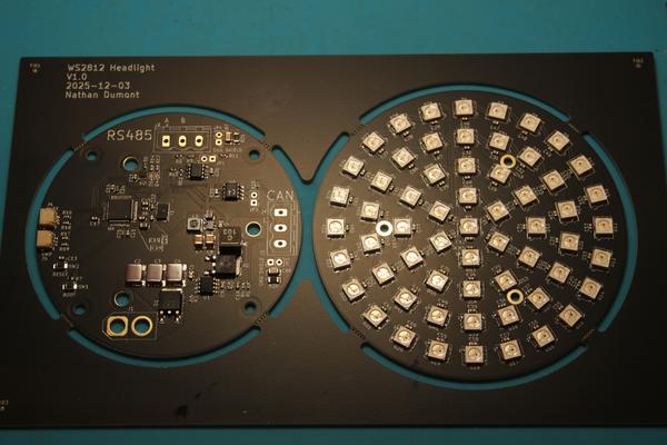
Once I had all the parts on hand I placed the stencil carefully over the board and spread solder paste. For DIY projects like this I use a low temperature paste to make it easier to build. The paste I've used has a bit of a tendency to make blobs but it does solder without getting so hot. I used an old plastic coffee loyalty card as a squeegey to spread the paste. The stencil from PCBWay worked well without any extra messing around.
With paste down it's best to move fast so I placed all the LEDs first and the capacitors next to them. I used a miniature hot plate to solder those parts down so I wouldn't risk knocking them while placing the control parts. I placed the control parts next and soldered them with the hot plate again. The MCU needed a little bit of hand rework but other than that the board soldered up easily. I added the pillars by hand with a soldering iron.
Test and firmware
The first test I did was just a straight power supply test. Everything was good, the 3.3V and 5V rails were very accurate and the current consumption was low. Getting the MCU up and debugging was a bit more of a chore. The version of OpenOCD from ST that I had installed to work on my last H5 project didn't recognise the MCU. After a bit of concern that I had more soldering issues I found a newer version of the ST fork of OpenOCD with support for my MCU. I've written a small test firmware to light the pixels and test they all worked. There's plenty more to do to add some more animations and to add controls and communication but at least it proves we can control each pixel.
The driver for the WS2812s is based on an SPI peripheral. There are lots of places the protocol is documented, essentially you need to provide a 1.2µs pulse, with 2/3 duty cycle for a 1 and 1/3 duty cycle for a 0. To achieve this I configured the PLLs in the H5 to make a bit period of 200ns (5MHz) and set it to send 6 bit words. This way I could send a 1 symbol by transmitting 0x3C and a 0 by sending 0x30. The H5's very flexible clocking and SPI peripherals made this setup easy, but the way the H5 transmits SPI made using it hard. When you start transmitting with the SPI peripheral there is about a 200ns turn-on time during which the MOSI line is high. This causes the most significant bit of the first pixel to always be a 1 which means it's always at least 50% green. To overcome this my code uses the low-level API and keeps the SPI FIFO full of zeros whenever there's nothing to send which keeps the bit periods fixed and the MOSI line low.
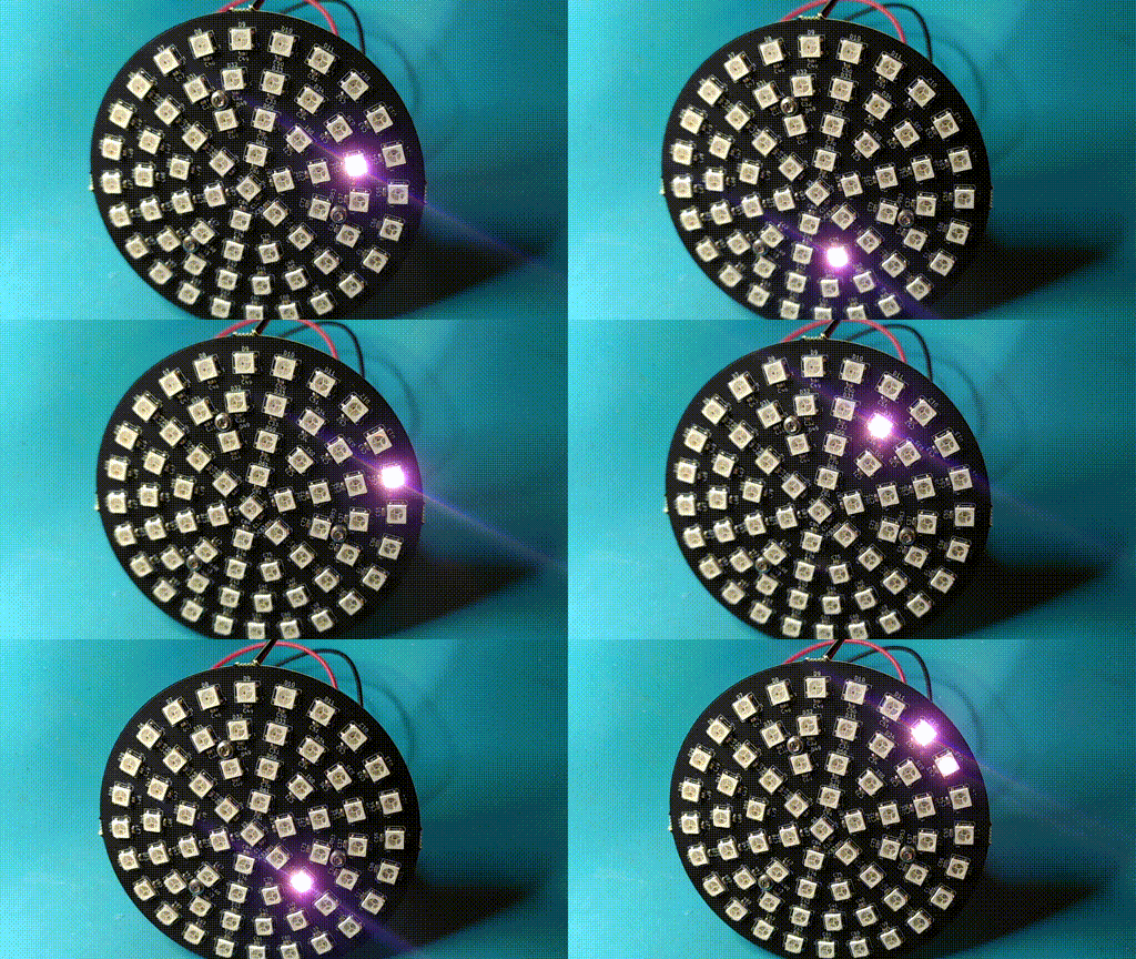
Pixel test: One pixel at a time to check they all work
Firwmare is on my GitHub
Comments
If you want to discuss this article you can reach me via email.
