Trimming Silk Screen on KiCad
Last updated: May 18, 2014, 3:03 p.m.
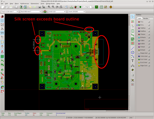
Sometimes when submitting boards for cheap panelised manufacture you need to keep all of the layers of the gerber file within the size of the PCB. In some boards I find there are bits of silk screen (e.g. connector outlines) which overlap the edge of the board. As far as I can see there's no way to limit the silk screen to the edges of the board by default, but I have a work around that might be useful.
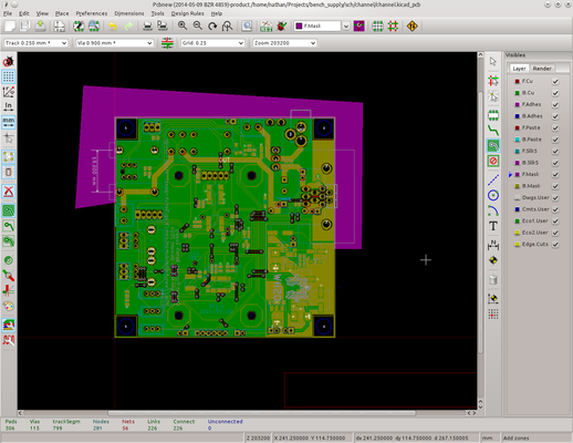
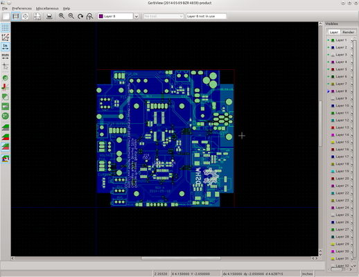
There's an option in the gerber plotting options "Subtract soldermask from silkscreen". My solution is to use this feature and draw a temporary soldermask fill zone surrounding the outside of the board. With the fill in place, just plot the silk screen layer with the option ticked. Remember to delete the fill again before plotting the soldermask layer, otherwise that will extend outside the area of the board instead of the silk screen.
Comments
If you want to discuss this article you can reach me via email.


