Nathan's Z80 Project Mark 2: CPU
Last updated: Aug. 26, 2009, 11:06 p.m.
The CPU in this system is a Z80 of course. There isn't much to this section in way of technical content, just a few explanations of what pins I've ignored and why really. I'm not using the RFSH pin as I'm using static RAM, I can't think of a reason to use this in a modern system, and can think of lots of reasons not to, DRAM is just too much like hard work if you ask me. I've not connected anything to halt as I didn't really have room on the board in the end, it is often handy to put an LED on here (although it should be driven with a transistor as this pin can't sink/source much current). I've not used the non-mask-able interrupt so that's tied high to stop it going off by accident, the M1 line is not used in this simple system, so is left un-connected.
There are two interrupt sources in the system, the clock and the UART, so the interrupt signals are combined with a simple AND gate, (remember if you want a trigger on either one OR another active low signal you must AND them, likewise if you want a trigger only when one AND another are active you must OR them). The RESET line has a pull-down resistor on it. This makes sure that the Z80 is dormant until the PIC drives this line high, so if the PIC is reset or not running for some reason the Z80 is asleep. The BUSRQ and BUSACK lines are directly linked to the PIC so that it can request the use of the system bus without the Z80 clearing its registers.
Because I'm using a fairly large fan-out and a mix of TTL and CMOS in this system it is always wise to buffer the bus lines with some TTL capable chips (HCT or LS type preferably) that can drive more current than the Z80 alone. To make sure the outputs of these chips obey the same rules as the Z80's own pins the enable lines are driven by the BUSACK signal, inverted. This means that when the Z80 hasn't given away control of the bus, BUSACK is high so once inverted it provides the active low enable input to the bus drivers. Once the Z80 has signalled it does not need the bus (by setting BUSACK low) the drivers outputs all become high-impedance.
There's also a resistor pack attached to the data bus shown here. This is added because I found that the capacitance of the data bus is high enough to act as a fairly effective memory when working on the Mark 1 project. I could write to and read back data from memory addresses that were not physically within the system just because the bus held the voltages longer than the turn around time of the CPU. Adding a resistor pack ensures that any residual current is dissipated through these resistors and doesn't hang around too long.
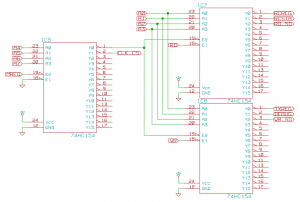
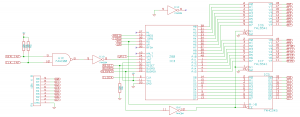
The decode logic for the IO bus is fairly simple, but provides full decode so all 256 address can be used. This was important as I intend to use this as a basis for developing peripherals. The top 4 bits of the IO address are fed into a 74HCT154 along with the IORQ signal as an enable. This provides 16 select signals to IO devices, the first IO device is further decode, the second is the clock which has 16 internal registers for configuration and date retrieval. The decode of the first address is continued with two more 154s which have the select from the first 154 as an input so they are only active when IORQ is asserted, the second enable comes from WR or RD to make two sets of 16 selects, each set either read or write only. These are used for buffers, latches or the UART's two read and write only ports. Two of these signals are combined back together to select the SD card interface provided by the PIC.
Datasheets
Z80 8 bit CPU 74HCT154 4 to 16 decoder
Comments
If you want to discuss this article you can reach me via email.